KF5N Radio Experimentation Site
QSE2DCEZ
This is the PCB for the QSE2DCEZ exciter module for the T41 “Software Defined Transceiver”.
The PCB was designed using the open-source design tool Kicad 8.
QSE2DCEZ uses SOIC package parts rather than TSOP for ease of assembly (easier to solder).
The QSE2DCEZ evolved from the original V011 design which remains the most recently published receiver module for the T41 Software Defined Transceiver.
Version 1.1 adds another inverter/buffer IC which decreases loading on the local oscillator input. This improves the quality of the quadrature quality in the higher bands.
A connector is provided to supply 5.0 volts and I2C interface to an Si5351 PLL module. This allows a more direct connection of the PLL output to the QSE2DC clock input. When this option is used, the PLL output from the T41 Main board is no longer required.
The goals of the QSE2DCEZ are to improve transmitter performance, and in particular, the performance in the 10 meter amateur radio band. Please note that the designer of this project does not own a laboratory full of expensive test equipment. There are no guarantees or other warranties of the performance of this transmitter module. What you see is what you get!
The Github repository for this board is here:
https://github.com/Greg-R/qse2/tree/qse2dcez
Gerber files for PCB fabrication are included in the gerbers folder. A PDF of the schematic (qse2dcez.pdf) is included for quick viewing of the circuit design in the doc folder.
QSE2DCEZ requires a simple modification to the Audio Adapter board. The modification is described below.
Please note that the components used in this design increase the cost compared to the original design. However, the board is easier to build. A link to a public Digikey BOM is included so that the prospective builder can evaluate the cost before proceeding.
Note that there is another version of this board which swaps the SIOC package parts with TSOP. Soldering TSOP parts is a little bit more difficult. This alternative version QSE2DC is here:
https://github.com/Greg-R/qse2/tree/main
Divide-by-2 versus Divide-by-4
The original QSE uses a divide-by-4 quadrature LO generator circuit. This is a robust circuit which produces high-quality quadrature local oscillator waveforms. However, the circuit has a trade-off and that is the requirement for VHF range frequencies in the higher amateur HF bands.
For example, transmission of a SSB signal at 28.510 MHz requires a frequency of:
28.510 MHz * 4 = 114.040 MHz
This frequency is applied to the quadrature generator which is composed of a dual flip-flop integrated circuit. The circuit is powered from the 3.3 volt supply.
The flip-flop device is a type 74AC74. The specification sheet is here:
https://www.ti.com/lit/ds/symlink/sn74ac74.pdf
The specification of interest, fclock with Vcc = 3.3 volts, is on page 4, and the maximum is 95 MHz. This is insufficient to support the 10 Meter band.
One page the same specification is shown for Vcc = 5.0 volts, and the maximum increases to 125 MHz. This shows a method to increase the frequency range, however, a matching 5.0 volt specified multiplexer must be used. A 5.0 volt multiplexer is in fact available at no cost penalty.
QSE2DCEZ resolves the high frequency problem by using a divide-by-2 quadrature circuit. The frequency is now:
28.510 MHz * 2 = 57.020 MHz
This is well within the frequency specification of the 74AC74 flip-flop IC even with Vcc = 3.3 volts.
Implementation of the Divide-by-2 Quadrature
Once again you don’t get something for nothing, and the divide-by-2 quadrature circuit requires a little more effort.
Divide-by-2 requires a clock signal and the inverted clock signal. This is easy enough to provide using an inverter integrated circuit:
https://www.ti.com/lit/ds/symlink/sn74lvc1g14.pdf
So providing the inverted clock signal is easy. However, one solution creates a new problem! The inverter creates a small delay in the inverted signal. This affects the quality of the quadrature. However, this is easy to compensate for. Simply add another inverter to the output to “match” the delays. So we have to add two these inexpensive devices in addition to the same flip-flop device used by divide-by-4.
The divide-by-2 circuit was simulated and found to produce acceptable quadrature.
For optimal quadrature circuit performance, the coaxial cable between the Main board and the QSD2 should be as short as possible.
Why is it called QSE2DCEZ?
QSE2DCEZ -> “Quadrature Sampling Exciter Two Direct Coupled”
The “EZ” is due to the substitution of SOIC package parts for ease of assembly.
The circuit is what is called an “IQ modulator”. Watch this video to learn more:
Note that in the above video the IQ modulator is assembled from double-balanced diode ring mixers. This is another way to implement an IQ modulator. The QSE2DCEZ is a sampling type circuit topology. From a “black box” perspective, the two circuits perform the same function.
Carrier Nulling
One of the problems with the original QSE is that it can have excessive carrier leakage. This tendency to pass the carrier to the output gets worse at higher frequencies.
Why is carrier leakage bad? At some point if the carrier is high enough, the op on the other end will be able to notice it. The demodulated signal will be distorted. The received signal will be unpleasant to listen to. A similar problem will occur with digital transmission. The error rate will increase as the carrier leakage increases. Carrier leakage is one of several “impairments” which happens with IQ modulators. Another example of an impairment is the sideband suppression.
Sideband suppression can be compensated for by using DSP techniques. This is done by small phase and amplitude offsets in the I and Q signals applied to the inputs of the IQ modulator. This is done intentionally and is how the T41 calibration process works.
“Direct Coupled” is a significant difference from the original QSE. The original QSE is capacitively coupled. This makes it impossible to perform carrier nulling. The connections between the I and Q DACs are direct coupled. There are no blocking capacitors. This makes it possible to perform carrier nulling (calibration).
A simple modification to the Teensy Audio Adapter board is required, as that circuit includes blocking capacitors. The coupling capacitors are removed and replaced with 0 ohm jumper resistors.
Software Modifications for Divide-by-two
Another complication of the divide-by-two is that the circuit must be properly reset prior to application of the local oscillator signal. If the reset is not executed, the circuit may produce inverted quadrature or it may not function at all.
Thus a reset signal must be provided to the QSD2 board.
This turned out to be easy to implement. The QSD is designed to be powered from the 16 pin ribbon cable which connects all of the radio’s modules together to a common power supply. There are unused pins, and one them is used to provide the reset signal. A single wire is tacked onto the back side of the Main board, between a GPO pin of the Teensy and the unused pin on the 16 pin IDC connector. That is all!
The software modification is equally simple. The reset is toggled prior to the application of the local oscillator signal at radio power-up. That is all that is required to guarantee that the divide-by-2 quadrature circuit is properly initialized. This is a common and practically universal requirement for digital circuitry.
There is no change to the calibration code. In fact, the divide factors can be mixed. For example, a divide-by-2 QSD2 can be used with a divide-by-4 QSE. As long as the correct divide factors are used, calibration will work perfectly.
Software Modifications for Carrier Calibration
Carrier calibration requires the addition of a new item to the calibration menu: “Carrier Cal”. The calibration process works precisely the same as the undesired sideband calibration. The rotary encoder is rotated to find a “null” as shown in the display, and then the channel is switched, and nulling is done on that channel. It may be necessary to switch back and forth between channels to find the optimum carrier null.
Calibration numbers are saved to the EEPROM non-volatile memory at the conclusion of the process.
T41EEE Arduino Sketch with Special Features for QSE2DC
The Arduino sketch designed to work with QSE2DC is located here:
https://github.com/Greg-R/T41EEE
You will need to modify the file “MyConfigurationFile.h”. The default code looks like this:
// Set multiplication factors for your QSD and QSE boards.
#define MASTER_CLK_MULT_RX 4
#define MASTER_CLK_MULT_TX 4

// Uncomment this line for QSE2.
//#define QSE2
Assuming you are using both QSD2 and QSE2DCEZ, you should change the code to this:
// Set multiplication factors for your QSD and QSE boards.
#define MASTER_CLK_MULT_RX 2
#define MASTER_CLK_MULT_TX 2

// Uncomment this line for QSE2.
#define QSE2
If you are using the Si5351 module, there is another line to uncomment:
// Uncomment this line if using an external PLL module.
#define PLLMODULE
A Summary of Methods to Extend the T41 Frequency Range
The T41 is an “Experimenter’s Platform”, and there is no right or wrong way to solve a problem. It is the experiment; the journey of discovery and amateur radio fun and adventure is the destination!
Here are a few ways to experiment with T41 frequency range expansion:
- Change the bias voltage on the 74AC74 from 3.3 volts to 5.0 volts. Change the multiplexer IC to a part specified for 5.0 volt operation. This changes increases the frequency response of the flip-flop device.
- Change the 74AC74 to a device specified for higher frequencies while leaving the bias at 3.3 volts. The device is the 74LVC74. The specification sheet is here: https://assets.nexperia.com/documents/data-sheet/74LVC74A.pdf.
- Change the divide-by-4 circuit to the divide-by-2 circuit as described above. This circuit is slightly more complex, however, it has large margin to the upper frequency limits of the components at 10 meters. 6 meter operation may be possible. There is no known low-frequency limit to the divide-by-2 (or divide-by-4) circuit.
- The T41 V012 design generates quadrature using an internal phase-shift circuit, such that one clock output is in-phase
and another clock output is shifted by 90 degrees. This is directly applied to the multiplexing (demodulator) device,
and thus this circuit is very simple. This also exploits the maximum upper frequency range of the Si5351 phase-lock-loop IC.
On the other hand, this introduces a low frequency limit and it may not be possible to cover the LF and VLF amateur bands with this scheme.
Other Changes to the QSE2DCEZ Circuit Design
The QSE2DCEZ exciter module circuitry is almost entirely revised compared to its ancestor the V011 QSE.
Pi RF Attenuator
A Pi resistive attenuator is added on the output of the QSE. This can be adjusted depending on the gain of the power amplifier. The nominal design has about 3 dB of attenuation.
Output Transformer
The original V011 modulator circuit uses a hand-wound toroidal output transformer with a tapped primary. QSE2DCEZ changes to a ready-made surface mount transformer which is untapped:
https://www.minicircuits.com/pdfs/ADT1-1+.pdf
Using this ready-made transformer means no toroid winding! However, it is expensive: US$4.02. Note that other transformers with the same footprint may work in this circuit. The middle pads are open-circuited which means even tapped transformers can be used.
Differential Operational Amplifiers with Low-Pass Filter
Fully differential operation amplifiers replace the op-amps from the V011 circuit. This is intended to improve the symmetry and balance of the modulator circuit, thus improving performance.
A low-pass filter is implemented using the differential amplifiers. This is a significant simplification, as a separate low-pass filter is not required.
A disadvantage of the differential amplifiers is higher cost. The AD8137 device cost is US$4.12 Quantity 2 are required.
Power Supply Decoupling and Regulators
The power supplies routed through the 16 wire ribbon cable are prone to noise, most likely from the Main board. Regulators for the three required voltages include low-esr bypass capacitors. This will provide clean bias sources to the modulator circuit.
Connectors
The I/Q output connector is changed to surface mount. The RF SMA connectors are the same, or they can be changed to right-angle connectors to improve coaxial cable routing. The 16 pin IDC connector is the same as the V011 board.
PCB Layout
The PCB layout was completed using Kicad version 8. This is an open-source tool, unlike the “Dip Trace” commercial product used to design the V010 and V011 series boards.
The layout in the quadrature generator and modulator areas was very carefully routed for maximum frequency performance. The QSE2DCEZ is approximately the same board size as V011, but there is unused area to add additional circuitry if desired.
The prototype PCBs were fabricated by PCBWay at a cost of US$1.00 each. Shipping was about US$25.00 for quantity 5 boards.
Bill Of Material (BOM)
A public Digikey BOM is here:
https://www.digikey.com/en/mylists/list/XQQB1BJVVE
Please note that specific parts may or may not be available when attempting to order. It is the responsibility of the builder to find subsitutes as required.
Build Tips
In general, QSE2DCEZ is easier to build than the original V010/V011 series boards. There are a few items to be aware of to avoid build errors.
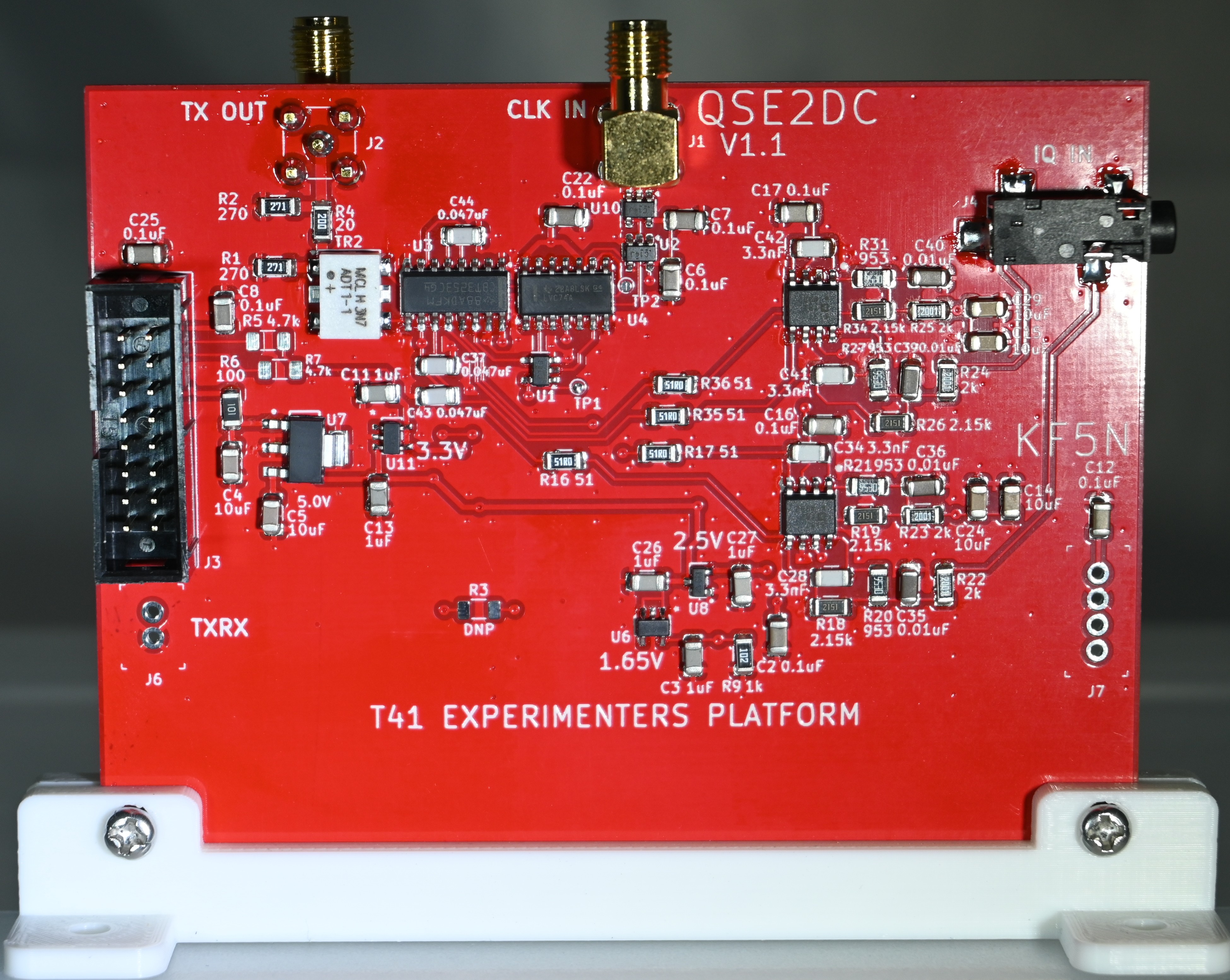
The most probable error(s) are incorrect orientation of the flip-flop, multiplexer, transformer, and differential amplifier devices. The pin 1 markings on the devices are very difficult to see. The transformer markings are easy to read; this should be clear in the photograph of the finished board.
Here are details on each part with regards to proper orientation of the board. The descriptions are viewing the top side of the board, with the “T41 EXPERIMENTERS PLATFORM” near the bottom of the board in normal left-to-right reading orientation.
Transformer TR2
The transformer TR2 should be placed with the “dot” at the upper left corner. If you are using the ADT1-1+, it appears to be symmetrical, so the orientation shouldn’t matter. However, other transformers may require a specific orientation.
74AC74 Dual Flip-Flop U4
Pin 1 should be in the lower left corner. This is marked with a small white dot on the PCB.
3253 Multiplexer U3
Pin 1 is at the upper right. Look for a small white dot next to pin 1.
Differential Amplifiers AD8137 U5 and U9
Pin 1 indicated with a dot on the PCB. Both parts are oriented the same, with Pin 1 towards the upper right. There is a dot on the parts to indicate Pin 1, however, it is very hard to see. The package is beveled on the Pin 1 side; this is easy to see.
Non-placed Parts
Don’t place R3. Placing this jumper implements shutdown of the differential amplifiers during receive. This feature has not been tested.
Don’t place J7, R5, and R7 if you are building the board as a drop-in replacement for the original V10/V11 boards. J7, R5, and R7 are to be used with the T41-2 Main Board. These components are used with a cable to route power and the I2C bus to an Si5351 module. There are photos of this in the “Dual Bracket” page. Please note also there is a problem with the I2C bus in version V1.1 of the QSE2DCEZ PCB. This is easily fixed as described below.
The two-pin header J6 can be optionally placed if it is convenient to route the TXRX signal from the QSE2DCEZ board.
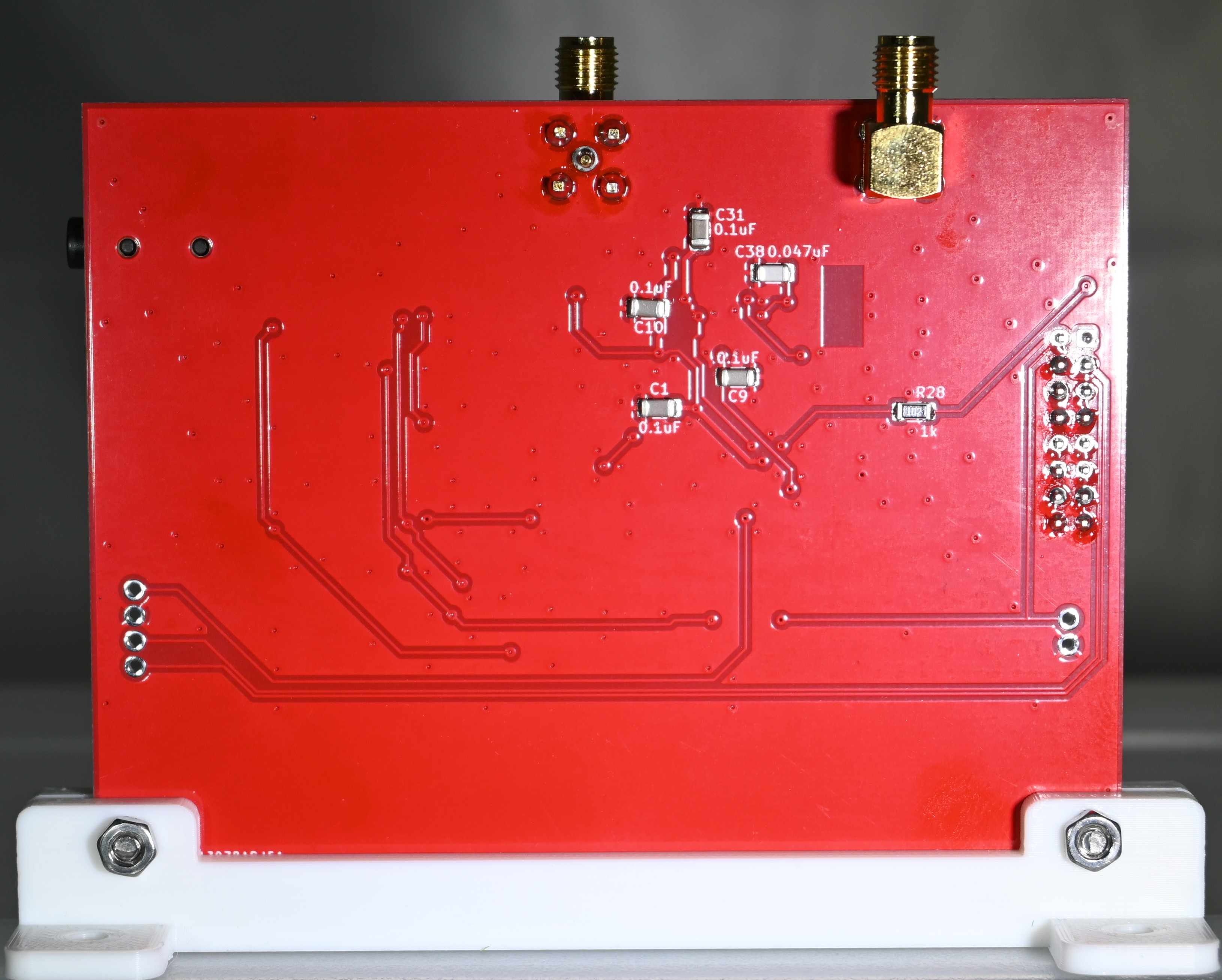
Bottom Side Parts
There are 5 capacitors and 1 resistor on the bottom side of the PCB. These should be soldered last. I was able to use a hot air gun without any problems with the top-side components desoldering.
SMA Connectors
Take a good look at the placement of the board in your T41 radio. You will want the SMA connectors of the QSE2DCEZ in the orientation for easy coaxial cable routing. I used 90 degree connectors as this was the easiest for extensive testing, but not necessarily the best for permanent installation. Also, you may choose to put the SMAs on one side or the other for optimal cable routing.
An investigation is underway to integrate an Si5351 local oscillator board with QSD2 and QSE2DCEZ. This will require a particular orientation of the local oscillator SMA connectors.
Please note that the cable from the Main board to J1, which is the transmit local oscillator, should be as short as possible.
High Resolution Photos of QSE2DCEZ
Links to photos of a fully constructed QSE2DCEZ follow. Please note that this board has some small differences compared to the published design files. Click on the image for the high resolution view.
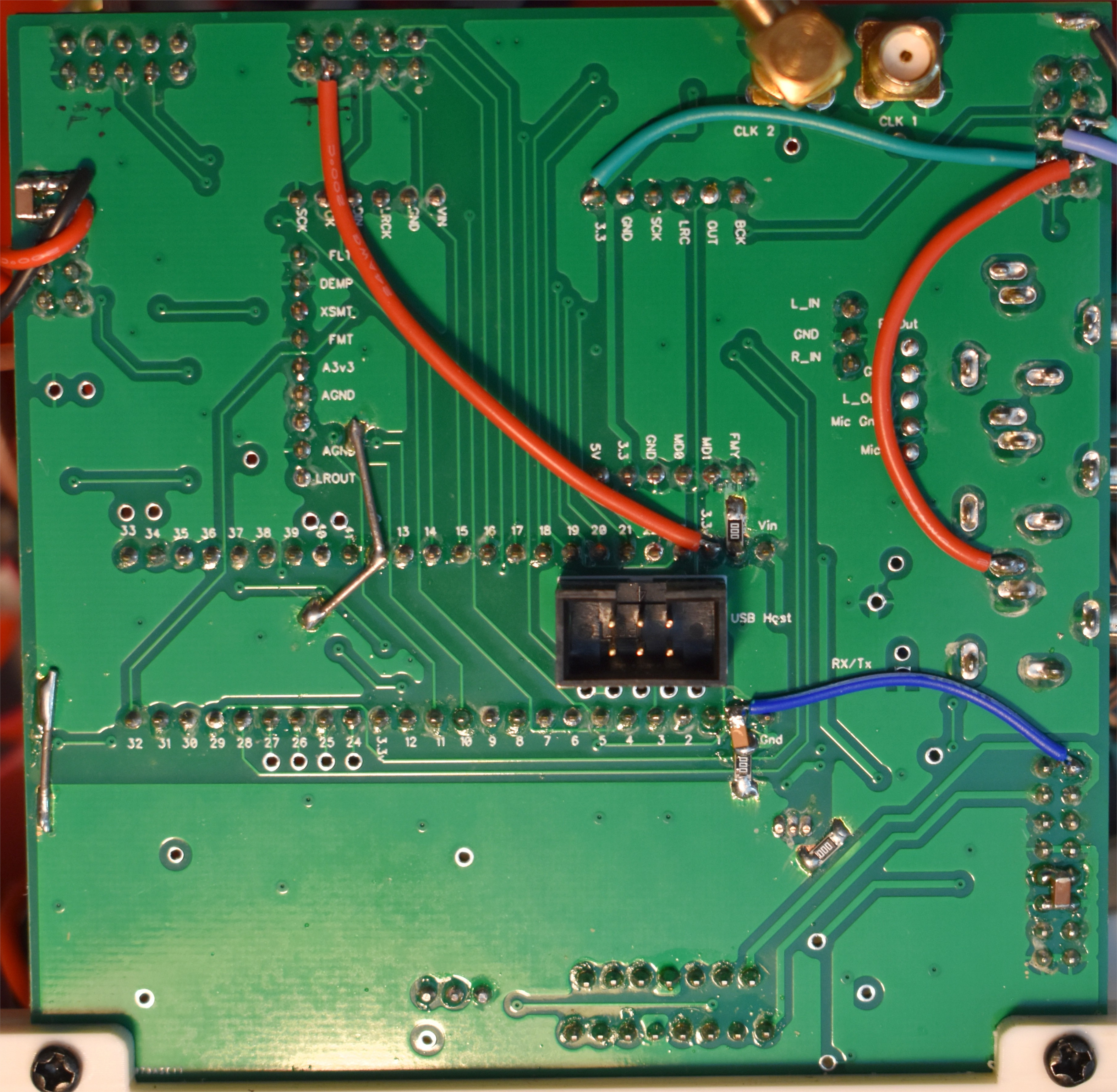
Main Board Wire for Flip-Flop Reset
A wire needs to be added to the original V10/V11 Main Board (not required for T41-2 Main Board) for resetting the dual flip-flop at power on. The wire is connected to pin 0 of the Teensy. Note that I also added a shunt bypass capacitor to ground. A zero-ohm resistor was required to reach ground. The other end of the wire connects to pin 1 of the 16-pin IDC connector. It might be better to tack the bypass connector to that end of the wire. In any case, be careful while soldering the wire because it is directly connected to the Teensy. Follow good ESD procedures to make sure the Teensy is not damaged. Here is a high resolution image of the Main board. The reset wire is blue.
I2C Fix for V1.1 QSE2DCEZ PCB Error When Used with T41-2 Main Board
There is a reversal of the SDA and SCL I2C bus wires in the V1.1 QSE2DCEZ PCB design. This happens at connector J7, which routes power and I2C bus to an Si5351 module. Fortunately, this is easily fixed by swapping wires in the cable which connects the QSE2DCEZ board to the Si5351 module. A picture is worth a thousand words, so here is a picture:
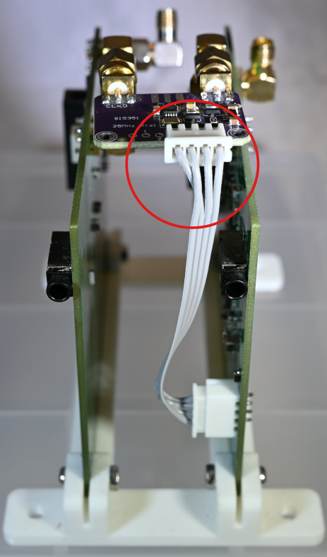
As shown in the photo, the first and second wires on the left are swapped. This is easily accomplished in the build of the cable by simply inserting wire #1 into connector slot #2 and wire #1 into connector slot #1.
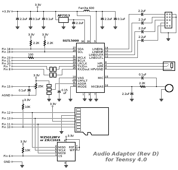
Modification of the Teensy Audio Adapter Board
The Teensy adapter board is described here:
https://www.pjrc.com/store/teensy3_audio.html
The T41 uses the left and right line-out channels for I and Q quadrature modulation. The schematic is here:
https://www.pjrc.com/store/schematic_audio4.png
Left and right line-out channels are from pins 11 and 12 of the SGTL5000 codec IC. Note the blocking 2.2uF capacitors. These blocking capacitors must be replaced with 0 ohm jumpers. These are standard surface-mount jumpers of size 0603 (1608 metric).
Here is a photo of an unmodified Audio Adapter board:
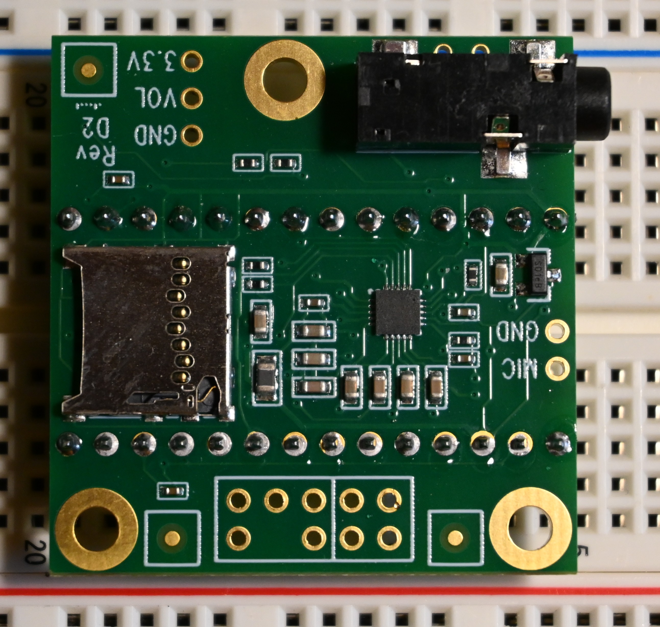
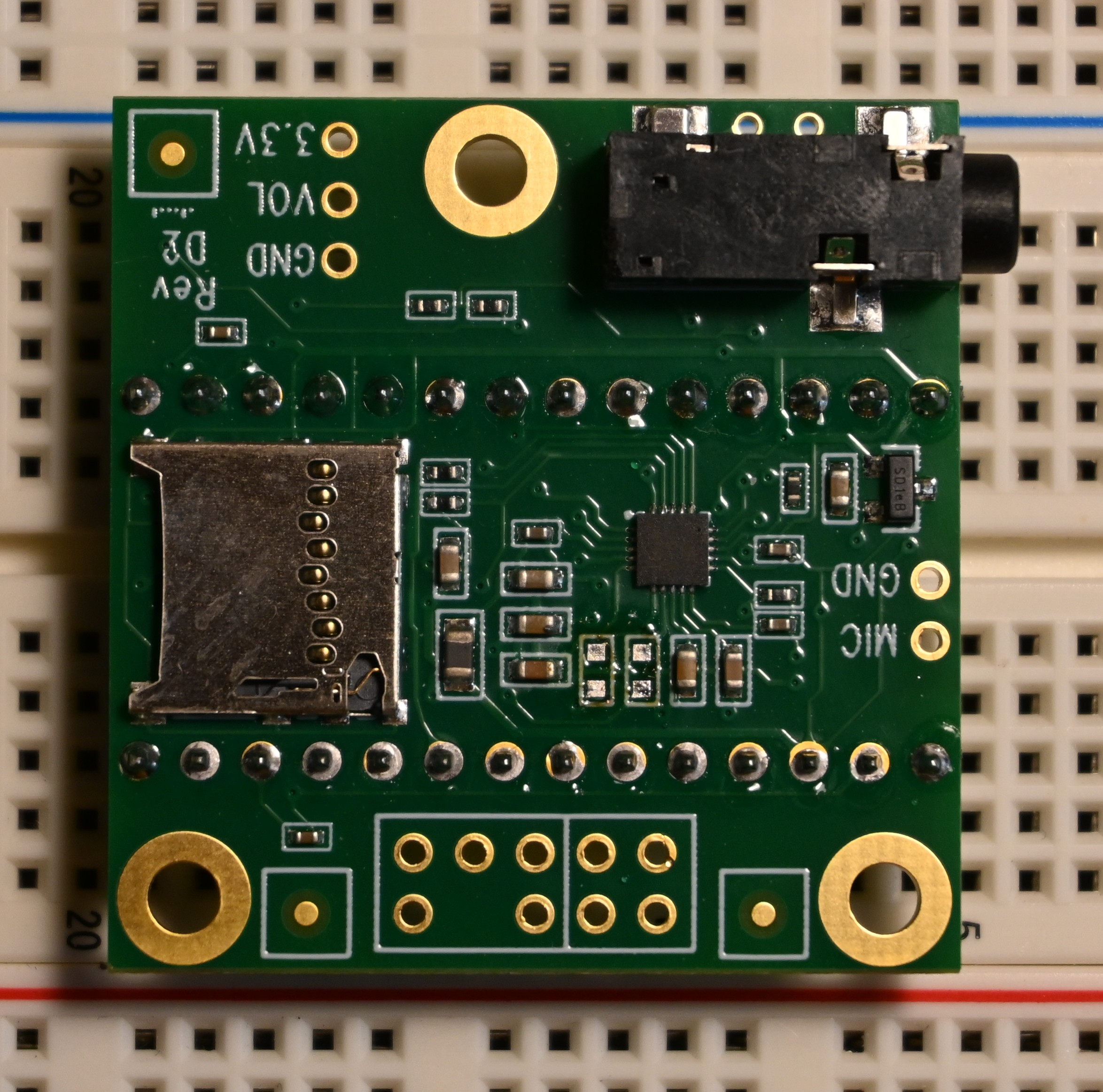
In the photo you can see 4 capacitors below the square IC package. The 2 capacitors to be replaced are the ones on the left. This can be seen clearly in this photo showing the capacitors removed:
After soldering the 0 ohm jumpers, the board looks like this:
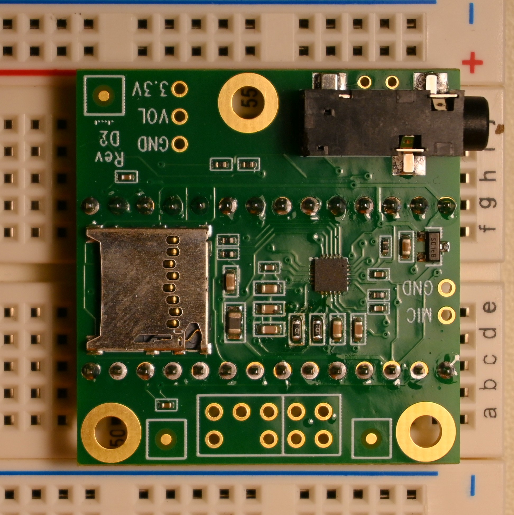
Note that the Audio Adapter board will continue to work with the original QSE boards, as they have their own input blocking capacitors.
References and Further Reading
The QSE2DCEZ is an attempt to integrate the best circuits from several sources into a high-performance HF exciter module. Here is a list of sources which inspired the design of the QSE2DCEZ:
- “Digital Signal Processing and Software Defined Radio, Theory and Construction of the T41-EP Software Defined Transceiver”, by Albert F. Peter, AC8GY, and Dr. Jack Purdum, W8TEE. This is the ultimate resource for builders of the T41 Software Defined Transceiver: https://www.amazon.com/Digital-Signal-Processing-Software-Defined/dp/B0F5BDQZW3
- “A Software Defined Radio for the Masses, Part 4” by Gerald Youngblood, AC5OG. This shows the circuit for the double-balanced modulator circuit and the use of instrumentation amplifiers on the output circuit. https://www.arrl.org/files/file/Technology/tis/info/pdf/030304qex020.pdf
- The Rod Gatehouse 2022 transceiver website: https://ad5gh.wordpress.com/2022-sdr-transceiver/ Rod took the original T41 SDT design and evolved it into a high-performance digital mode radio. Excellent circuit upgrades!
- “The Lentz Receiver: Tayloe Evolved” by H. Scott Lentz, AG7FF. An interesting discussion of several design features of the “Lentz Receiver” which improve the performance of the typical “Tayloe Detector” style HF receiver. Some of these ideas also apply to modulators. https://www.arrl.org/files/file/QEX_Next_Issue/2023/05%20may-jun%202023/05%202023%20TofC.pdf