KF5N Radio Experimentation Site
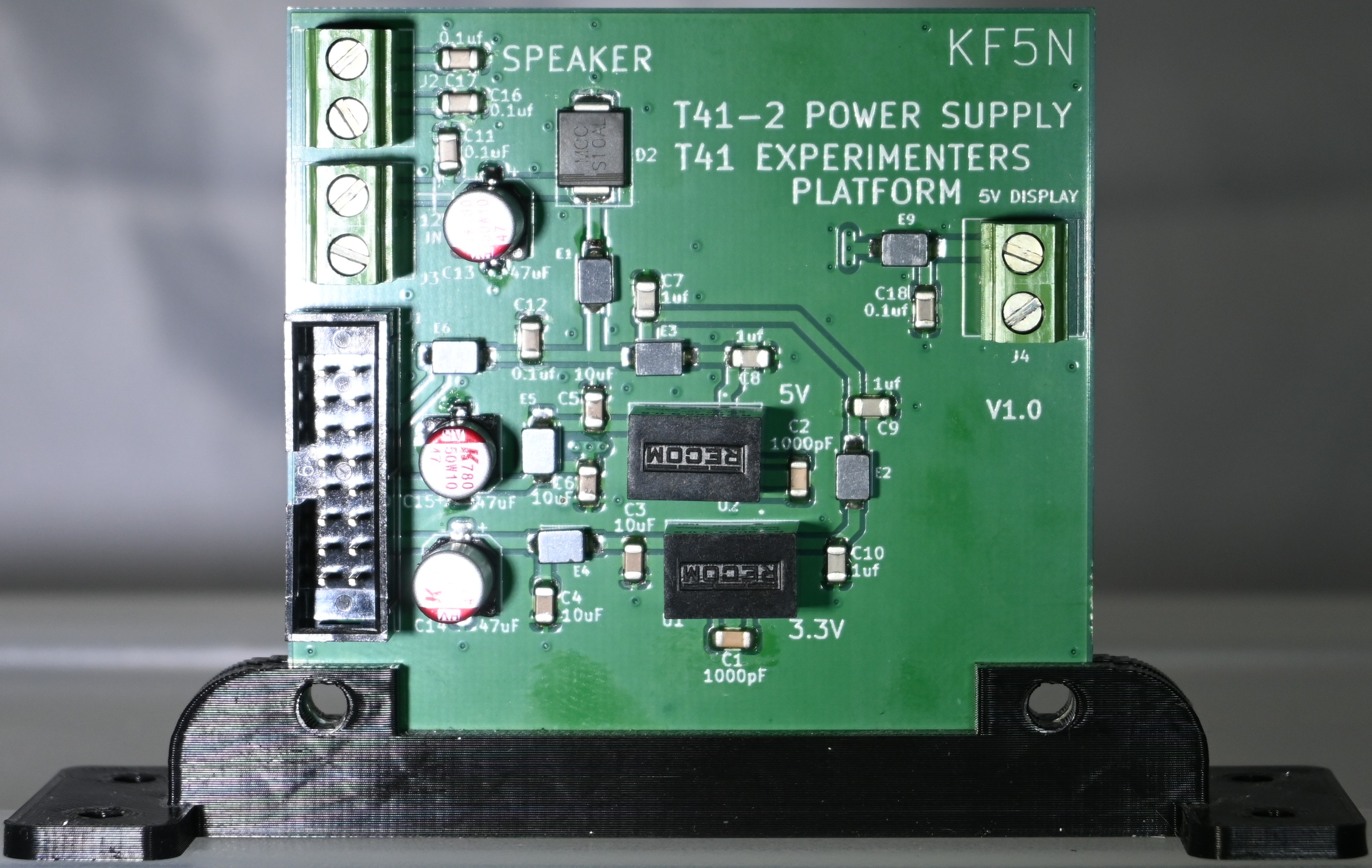
T41-2 Power Board
T41-2 Power Supply Module Version 1.0
This is the PCB for the improved Power Supply module for the T41 “Software Defined Transceiver”. The PCB was designed using the open-source design tool Kicad 8. The github repository is here:
https://github.com/Greg-R/T41-2_Power
The primary documentation for the T41 is the book “Digital Signal Processing and Software Defined Radio: Theory and Construction of the T41-EP Software Defined Transceiver Third Edition” by Albert Peter and Jack Purdum. The book is available here:
https://www.amazon.com/Digital-Signal-Processing-Software-Defined/dp/B0D25FV48C
The goal of the T41-2 Power supply module is to decrease current drain and dissipated power.
The original V10 power supply uses linear regulators for the 3.3 and 5.0 volt supplies with +12 volts input.
This dissipates a large amount of power in the regulators. The regulator devices get very
hot! This excess power dissipation increases the receiver current drain by a factor of two
compared to the T41-2! That is a serious problem when operating portable from a battery supply.
The vast majority of the T41 current drain during receive is due to the Teensy and the display. As the T41 evolves, more features included in the software means Teensy power consumption is going to increase. Also some builders are planning to use larger displays, thus increasing current drain and regulator dissipation even more. Watch out, your fingers are in danger!
The T41-2 Power Supply solves this problem by using the ingenious switching power supply modules by Recom:
https://recom-power.com/pdf/Innoline/R-78CK-0.5.pdf
A concern is noise and interference generated by the switching power supply circuits. All modern radios use switching power supplies and deal with these problems via appropriate PCB layout and decoupling. The T41-2 Power Supply is adequately decoupled, and testing so far has not revealed detectable noise from the switching circuits. Other circuits in the radio, primarily the Teensy and especially the display, tend to dominate the internally generated noise.
5 Volt Display Power Output
Another noise reduction feature of the T41-2 Power Supply is the +5 volt output for the display. Past experiments have demonstrated a reduction in receiver noise by switching the display to 5 volts and routing the 5 volt supply directly to the display rather than through the Main board. If this is attempted, the builder is advised to refer to the display’s manual to understand the change necessary to power the display from 5 volts rather than the as-shipped 3.3 volts. A means of routing the 5 volts to the display must be devised, which means adding wires and cutting the 3.3 volt supply from the Main board.
Gerber Files and PDF Schematic
Gerber files for PCB fabrication are included in the gerbers folder:
https://github.com/Greg-R/T41-2_Power/tree/main/gerber
A PDF of the schematic (T41-2_Power.pdf) is included for quick viewing of the circuit design:
https://github.com/Greg-R/T41-2_Power/blob/main/doc/T41-2_Power.pdf
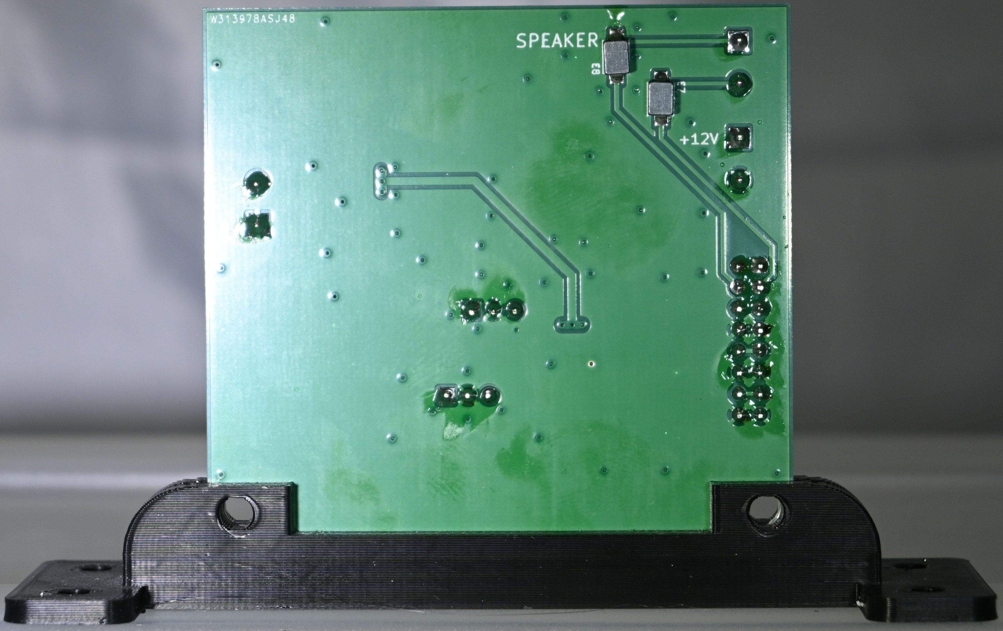
Speaker Output Terminal
A convenience feature of the board is a terminal for the speaker outputs. The speaker output from the Main board is routed via the 16-pin ribbon cable. However there was no plug or jack connected to these wires. Since the board has the common 16-pin connector, it is possible to route the speaker outputs to a terminal. This is an improvement, as the board can be removed from the radio without having to unsolder the speaker wires.
Please note that this feature is for V10/V11 and 4SQRP boards only! If using the T41-2 Main Board, do not place E7, E8, C16, C17, and J2.
Hardware Modifications
If you don’t want to convert the display to 5 volts, the board will drop-in. Please refer to the display documentation for 5 volt conversion instructions if you desire to make this modification. You will have to solder wires to either the Main board or display in order to connect to the 5 volt output of the power supply.
There is no modification required to the software.
PCB Layout
The PCB layout was completed using Kicad version 8. This is an open-source tool, unlike the “Dip Trace” commercial product used to design the V010 and other T41 boards.
The prototype PCBs were fabricated by PCBWay at a cost of US$1.00 each. Shipping was about US$25.00 for quantity 5 boards.
Bill Of Material (BOM)
A public Digikey BOM is here:
https://www.digikey.com/en/mylists/list/PVESXUZZUA
Please use the special low ESR/ESL bypass capacitors as specified in the BOM. These parts improve the bypassing and decoupling of the switching power supply modules.
Build Tips
In general, T41-2 Power Supply is easy to build if you have experience with surface-mount components.
Speaker Output Terminal
The speaker output terminal circuitry is not used with the T41-2 Main Board! If using the T41-2 Main Board, do not place E7, E8, C16, C17, and J2.
Ferrite Beads and Large Diode
The circuit uses several large ferrite beads, and one single large surface mount diode. I was able to solder these using regular solder paste and hot air gun. It requires a little more “dwell time” to get these large parts soldered.
Surface Mount Electrolytics
It may be easier to use a soldering iron for the surface mount electroytics. I was able to use the hot air gun successfully. However, I did melt the plastic base on these parts a little bit. That didn’t cause any damage, apparently.
If you don’t plan to use a supply voltage above the standard 13.4 volts, the electroytic capacitors C10 and C9 should not be placed. However, if you want to experiment with higher voltages, use the electrolytics, and delete ceramic capacitors C2, C3, C12, and C13. Please note that operating this amplifier with a higher supply voltage has not been tested here!
3D Printed Bracket
The 3D printed bracket is the same as the original Power Supply bracket. I have a repository with many files for T41 parts:
https://github.com/Greg-R/SDT_Case_KF5N
Bottom Side Parts
There are a few parts on the bottom side. These should be soldered after the top-side SMDs. I was able to use a hot air gun without any of the top-side components desoldering.
Through-Hole Parts
Solder the 16 pin connector and the through-hole terminals last.
High Resolution Photos of T41-2 Power Supply
Links to photos of a fully constructed T41-2 Power Supply follow. Click on the photos for a high-resolution image.