KF5N Radio Experimentation Site
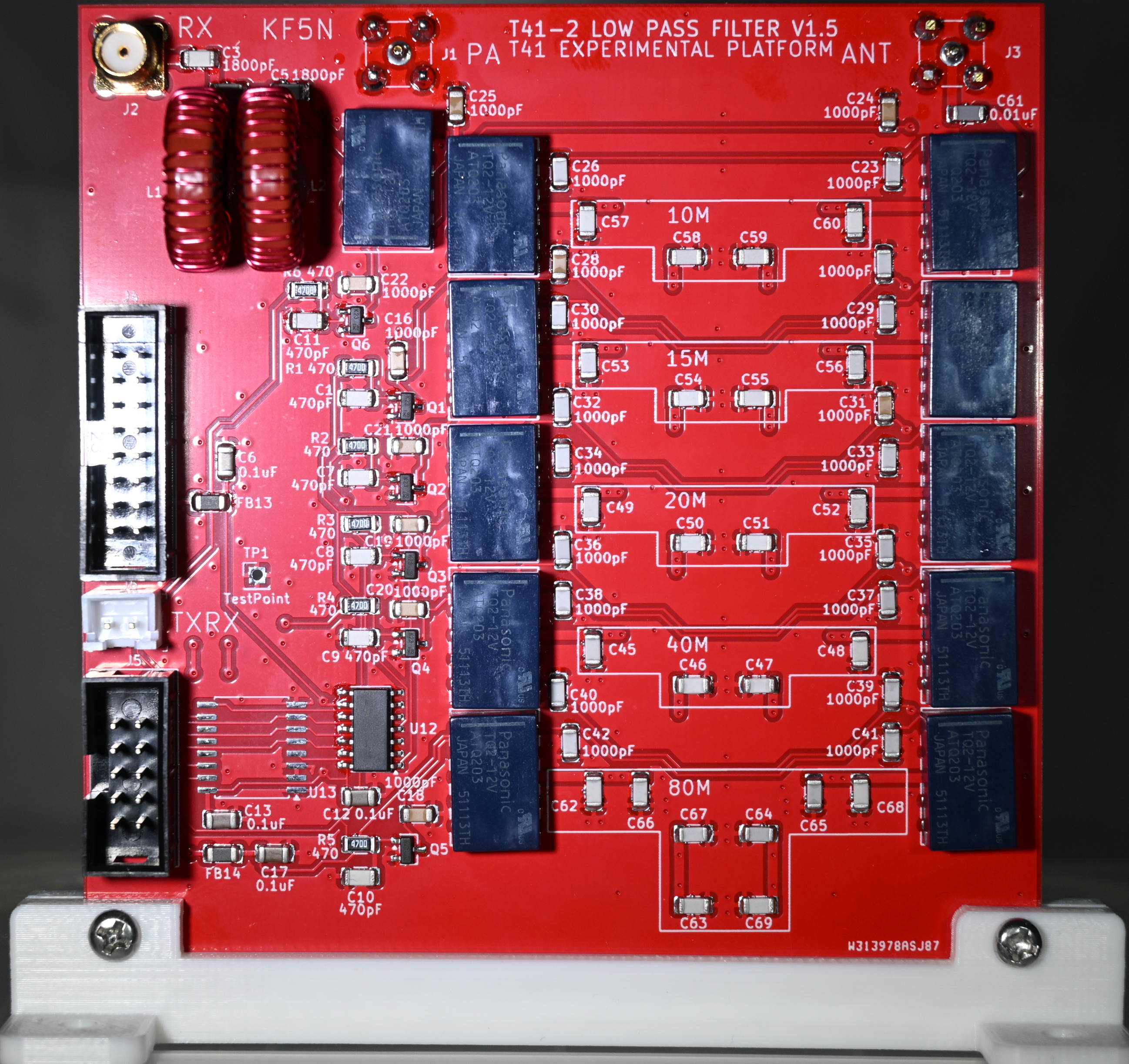
T41-2 Low Pass Filter
T41-2 Low Pass Filter Version 1.5
This is the PCB for the Low Pass Filter (LPF) module for the T41 “Software Defined Transceiver”. The PCB was designed using the open-source design tool Kicad 10.
The repository for this module is here:
https://github.com/Greg-R/T41_2_lpf
This filter is a functional replacement for the T41 Version 11 or 4SQRP Low Pass Filter (LPF) module. Some modifications to the V11/4SQRP Main Board are required as described below. The module is compatible with both the T41-2 and T41-3 Experimental Platform Software Defined Radio platforms without modification.
The primary documentation for the T41 is the book “Digital Signal Processing and Software Defined Radio: Theory and Construction of the T41-EP Software Defined Transceiver” by Albert Peter and Jack Purdum. The book is available here:
https://www.amazon.com/Digital-Signal-Processing-Software-Defined/dp/B0D25FV48C
The purpose of the LPF is to attenuate transmitter harmonics. This reduces the probability of interference. Transmitter harmonic levels are regulated by the FCC and other agencies. The module also includes a transmit-receive relay and a receive path high-pass filter to reject AM broadcast and other low frequency signals.
The LPF is inserted between the output of the Power Amplifier module and the antenna connector.
Gerber files for PCB fabrication are included in the gerbers folder. A PDF of the schematic (LPF-Filter.pdf) is included for quick viewing of the circuit design.
A look at the schematic:
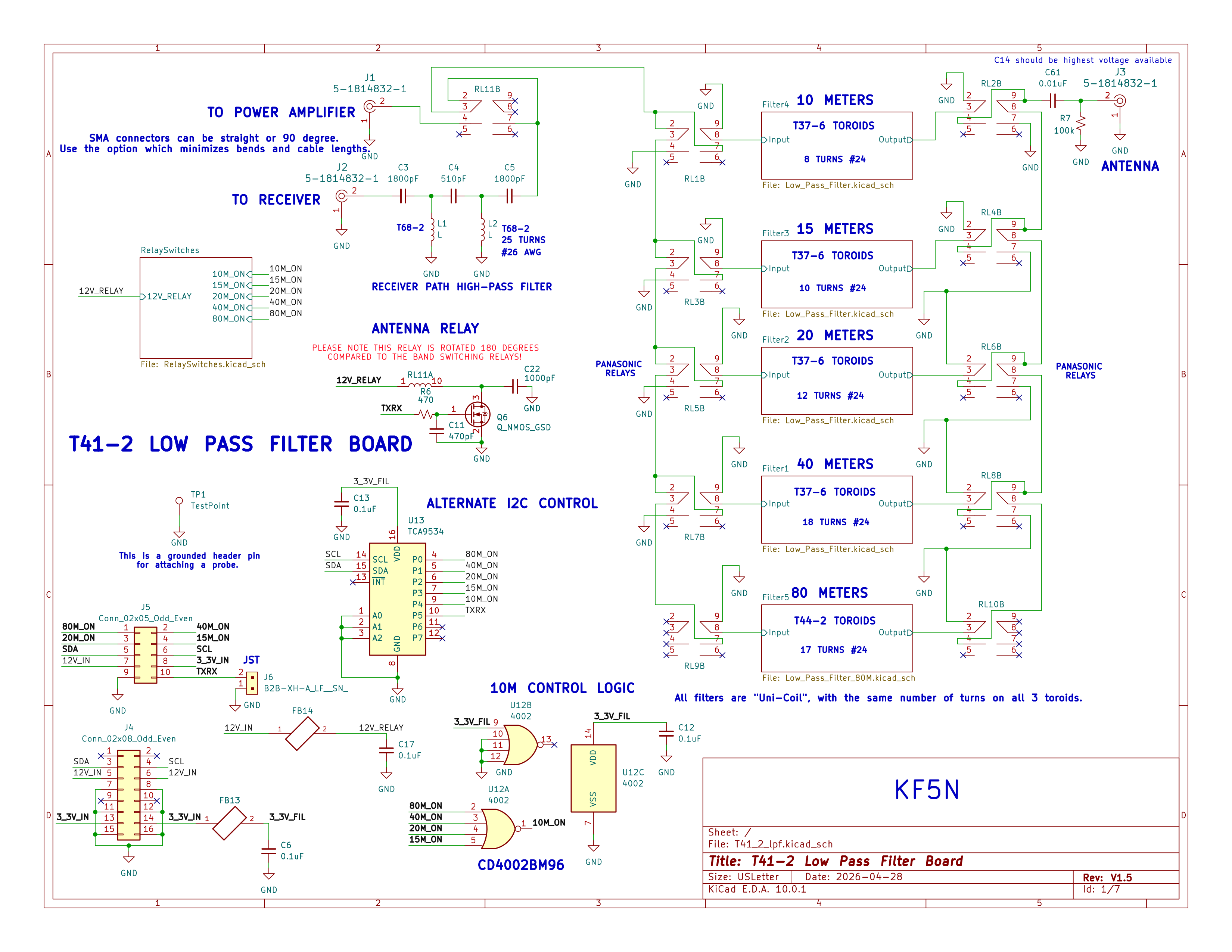
Please note that this is a hierarchical schematic. The filter switching and filter components are in separate sheets.
Hardware Modifications
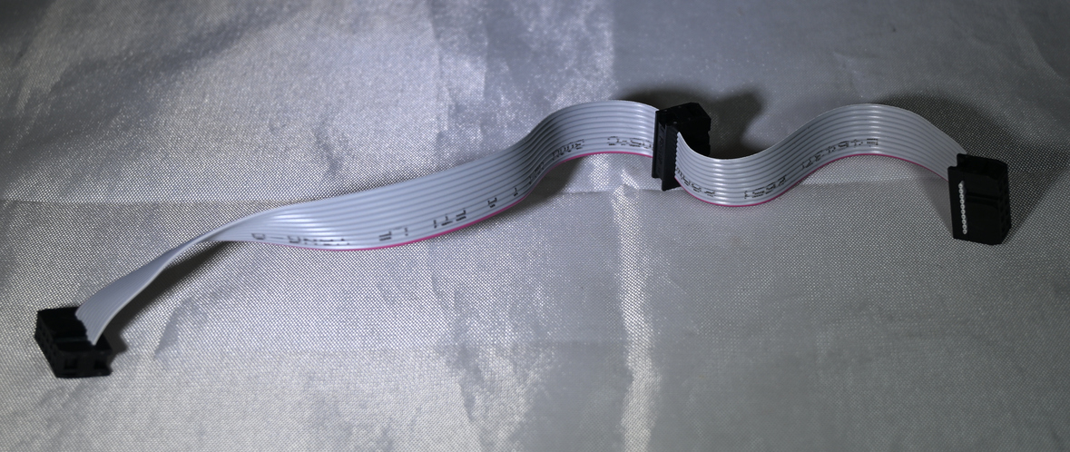
A new ribbon cable is required. The original T41 has a 10-wire cable which connects the Main board module to the Low-Pass Filter module. Since the QSE-Filter shares the same control signals, a new ribbon cable is required which routes from the Main board to the QSE-Filter, and then to the Low-Pass module. This type of cable is very easy to build and can be completed in five minutes or less.
Modifications for V11 and 4SQRP Radios
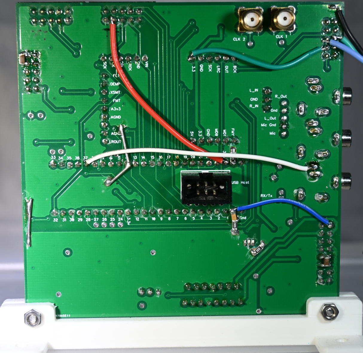
A wire must be added to the V10/V11 Main board to supply 3.3 volts to the module. This wire should be soldered to the
back side of the Main board from pin 8 of the “Bands” connector to a convenient source of 3.3 volts.
Looking at my modified Main board:
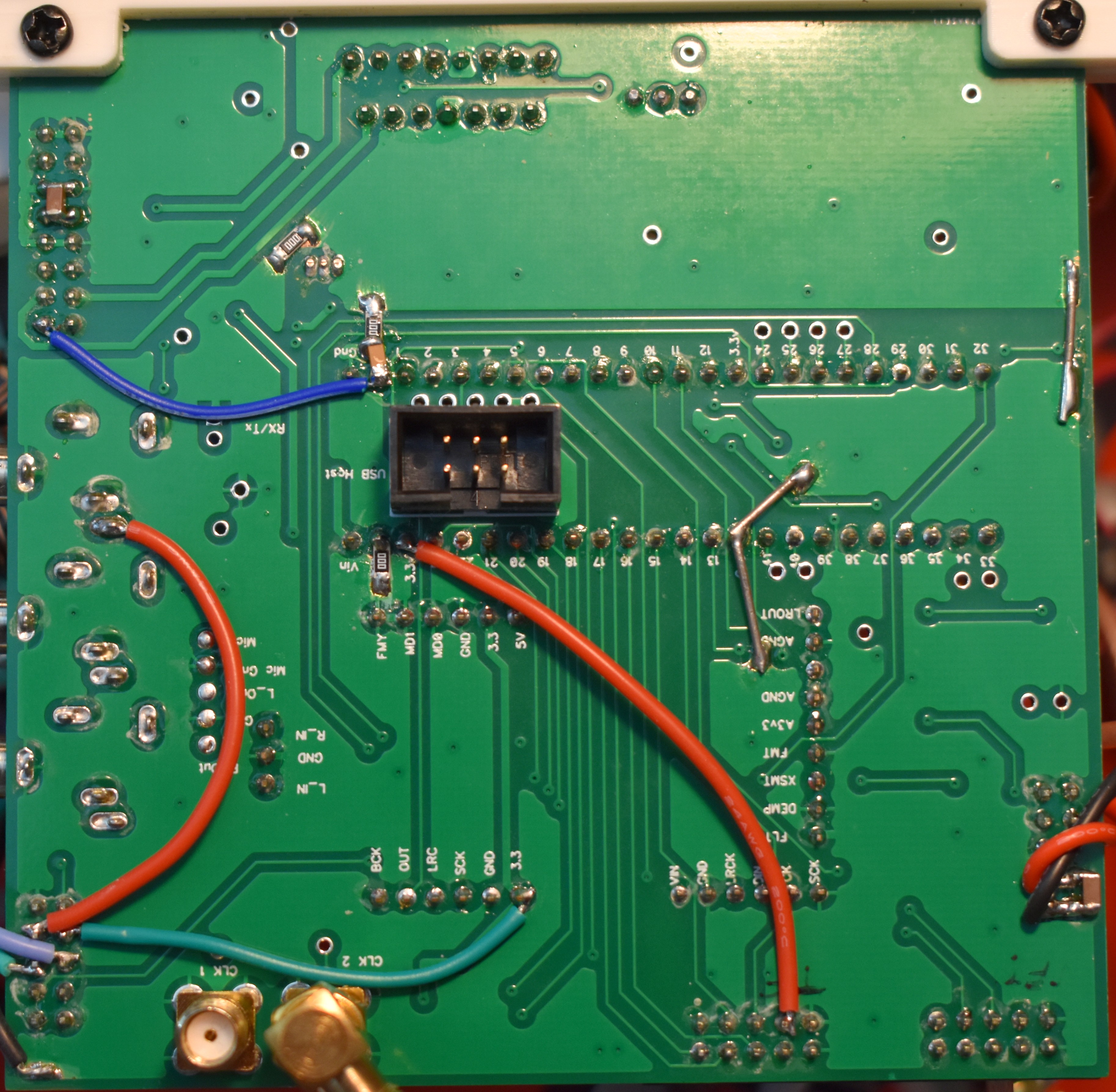
The green wire in the upper right area of the Main board routes 3.3 volts to the QSE-Filter via the ribbon cable. Note that this green wire is also required for the T41-2 LPF!
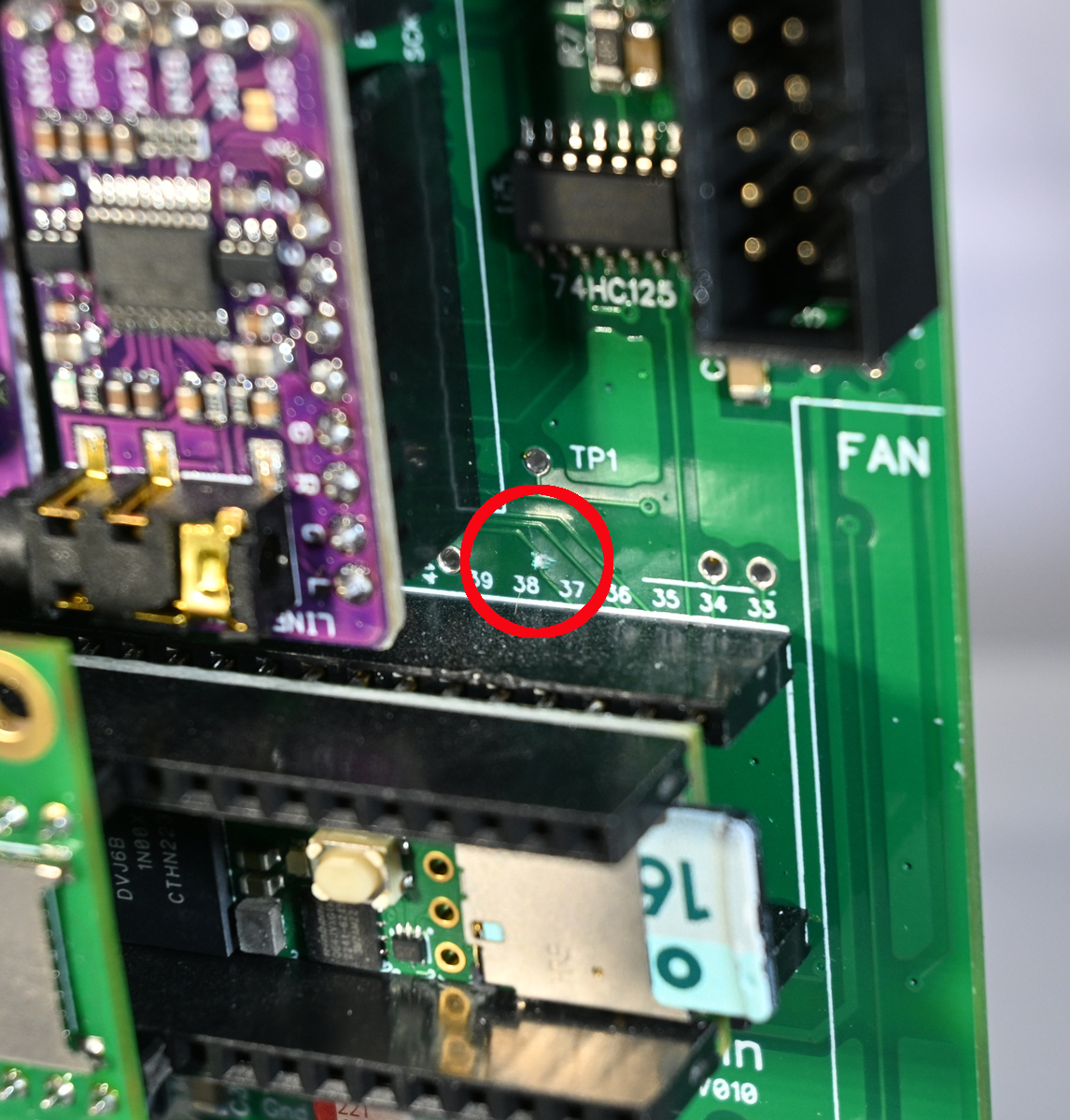
This next change is extremely important! If this is not done, there is potential for damage to the Teensy!
One trace on the V11 Main board must be cut! This is the trace which runs from pin 37 of the Teensy (as shown on the official schematic) to pin 7 of the 10-pin “Bands” connector. This circuit is the PTT control signal. This cut is shown in the following image:
The next change is required due to the above trace cut. This is a wire from pin 37 of the Teensy (as shown on the schematic) to the PTT GPO. This is seen as the white wire in the following photo:
These changes are not necessary for the T41-2 or T41-3 Main Boards. There is no modification required to the software.
Connector J4 with T41-2 or T41-3
The 16-pin connector J4 is not strictly required for use with the T41-2 or T41-3 Main Boards. J4’s only purpose is to supply 12 volts when the LPF is used with the V10/V11 Main Board. However, there are several ground wires in the ribbon cable and J4 is recommended to be used with all T41 versions.
Option for I2C Bus Control
The schematic shows an optional I2C bus control circuit. This circuit has not been implemented and tested yet.
PCB Layout
The PCB layout was completed using Kicad version 10. This is an open-source tool, unlike the “Dip Trace” commercial product used to design the V010 and other T41 boards.
The prototype PCBs were fabricated by PCBWay at a cost of US$1.00 each. The shipping cost is variable and is dependent on current tariff policy.
Bill Of Material (BOM)
A public Digikey BOM is here:
https://www.digikey.com/en/mylists/list/CP6Q6QQUW6
The toroids are not included in the above BOM. The T-37-6 (quantity 12) and T-44-2 (quantity 3) may be ordered from:
or from other reputable sources of RF components.
Filter Capacitor Values
This table shows the capacitor values in the five individual low pass filters. Be very careful to verify the correct value to be placed per this table. Note that 80 meters is unique in having 8 capacitors. The rest of the filters have 4.
The filter capacitors as specified in the BOM have a voltage rating of a minimum of 200 volts, and are NPO as available. This capacitors must have high Q factor. Be very careful if you substitute capacitors. Verify the specifications!
80 Meter Band Capacitor Values
| Designator | Value, pF |
|---|---|
| C66 | 1000 |
| C62 | 430 |
| C67 | 1000 |
| C63 | 1500 |
| C64 | 1000 |
| C69 | 1500 |
| C65 | 1000 |
| C68 | 430 |
40 Meter Band Capacitor Values
| Designator | Value, pF |
|---|---|
| C45 | 510 |
| C46 | 1100 |
| C47 | 1100 |
| C48 | 510 |
20 Meter Band Capacitor Values
| Designator | Value, pF |
|---|---|
| C49 | 300 |
| C50 | 560 |
| C51 | 560 |
| C52 | 300 |
15 Meter Band Capacitor Values
| Designator | Value, pF |
|---|---|
| C53 | 200 |
| C54 | 360 |
| C55 | 360 |
| C56 | 200 |
10 Meter Band Capacitor Values
| Designator | Value, pF |
|---|---|
| C57 | 150 |
| C58 | 300 |
| C59 | 300 |
| C60 | 150 |
To help during placement of the capacitors, download and print a copy of this PDF file:
https://github.com/Greg-R/T41_2_lpf/blob/main/doc/T41_2_lpf_cap_placement_guide.pdf
Build Tips
In general, the T41-2 LPF is easy to build if you have experience with surface-mount components. There are a few items to be aware of to avoid build errors and to achieve a high quality result.
There is a lot of hand soldering! Take your time and you will be rewarded with a working module.
The Best Build Order
The components should be soldered to the board in the following order. This is the easiest way to build the T41-2 LPF module.
- Surface mount components on front side of the PCB. I get good results using a hot plate.
- Relays. These are through-hole components. It is important to note that these relays must be installed in the correct orientation! The orientation is indicated by a line on the top of the relay housing, and there is a corresponding line in the silkscreen of the PCB. Note that relay RL11 is oriented in the opposite direction of the rest of the relays. Be very careful to double-check the orientation before soldering! These relays are difficult to remove once they are soldered to the PCB!!!
- The 2-pin JST connector which is the transmit-receive control. This connector is shorter than the connectors in step #4.
- 16 pin and 10 pin connectors. Both connectors are inserted from the front side. Note the “notch” indicated in the silkscreen! This is also something you should double-check, as these connectors are difficult to remove!
- SMA connectors. This is where you have options. The SMA connectors can be inserted from either the front or back side of the PCB. Also, straight or 90 degree connectors can be used. You should choose a configuration which minimizes the lengths of the SMA cables in your radio.
- The “surface mount” toroids. There are additional details on the toroid mounting technique below.
SOT Devices
This circuit uses a few SOT devices. These are generally well behaved even when using a hot-air soldering station. Be careful to not use too much solder on the pads. I had one short-circuit underneath one of the switches which caused high filter loss. A little bit of probing with a DVM revealed the short, and once the short was cleared the circuit worked as expected.
I have switched to using a hot plate for most of my surface mount soldering tasks. This works better than a hot-air soldering station in my experience. I use the hot-air station primarily for repair work or touch-ups, or in the case of where there are a few parts on the back side of a PCB.
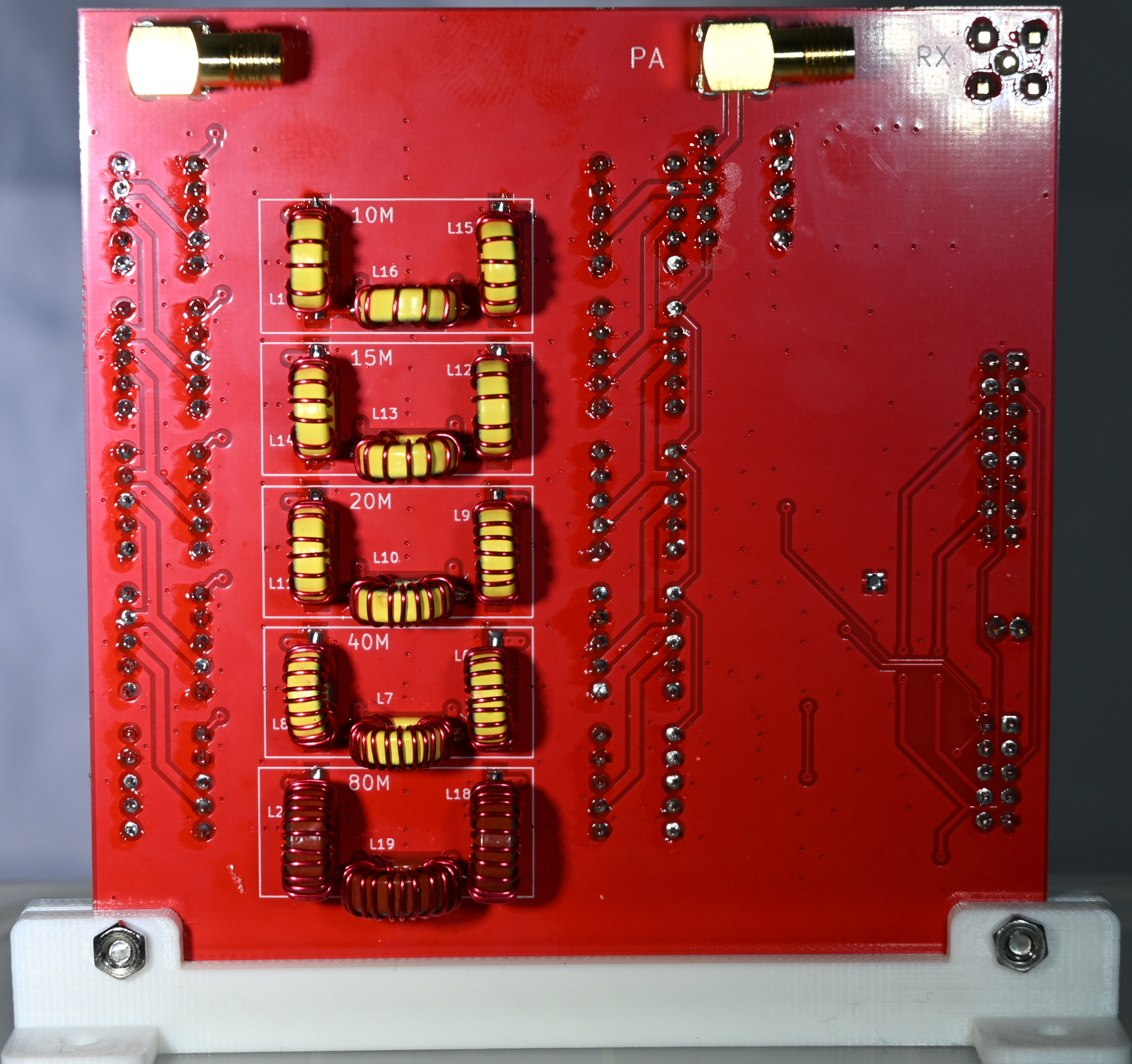
Toroids
This is what I consider the most difficult part of building the filter. Toroid winding! The toroid part numbers, wire gauge, and number of turns are shown on the schematic.
Try to space the windings evenly around the circumference of the toroid. However, the will be a gap in the windings at the wire ends. This is due to the “surface mount toroid” design of the PCB. That gap is part of the design, so don’t try to minimize it.
The toroids are “surface mounted”, meaning that there is a rectangular pad for soldering the wire end. I find this much easier to deal with than using through-holes, as soldering and re-soldering is much easier. Why resoldering? Because it may be necessary to add or remove a turn to get the frequency response lined up just right. Hopefully not, however, there are tolerances associated with both the capacitors and the toroids. The inductance will be a function of the toroid permeability, the number of turns, and also how you wound it. The frequency responses of the filters are designed to have margin, so hopefully all will line up and the frequency response of the filters will achieve the goal of a clean transmit spectrum.
Here is a photo of a “surface mount” toroid:
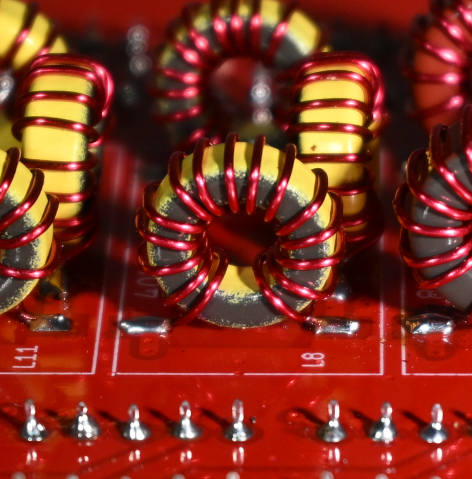
Note that the 80M filter uses T-44-2 toroids. The rest of the filters use T-37-6.
3D Printed Bracket
The T41-2 LPF Filter uses the standard T41 3D printed bracket. I have a repository with many 3D printer files for T41 parts:
https://github.com/Greg-R/SDT_Case_KF5N
The bracket is this part:
https://github.com/Greg-R/SDT_Case_KF5N/blob/main/bracket/Mounting_Bracket_KF5N.FCStd
SMA Connectors
Take a good look at the placement of the board in your T41 radio. You will want the SMA connectors of the QSE-Filter in the orientation for easy coaxial cable routing. 0 or 90 degree connectors are available (90 degree parts are on the BOM). Also, you may choose to put the SMAs on one side or the other for optimal cable routing.
High Resolution Photos of the T41-2 LPF
Links to photos of a fully constructed T41-2 LPF follow. Click on the image for a high-resolution view. Note that these photos show connector J4 in place. This connector is not required if used with the T41-2 or T41-3 Main Board.
Example Measured T41-2 LPF Frequency Responses
The following are measured frequency responses of the five filters. The markers are at the band edges, and there is also a marker at approximately -3dB and at the worst case harmonic frequency (2 times the low end of the band). The 15M and 10M filters also cover 17M and 24M respectively, thus there are more markers for those bands.


It is also interesting to look at the response from the antenna connector to the receiver connector. This path includes a high-pass filter which rejects AM broadcast and other low-frequency transmissions. The filter interacts with the lower bands, especially 80M and 40M, however, this is not a practical problem as these bands have high atmospheric noise. Here is a plot of the frequency response of the 10M path, which has less interaction with the HPF:

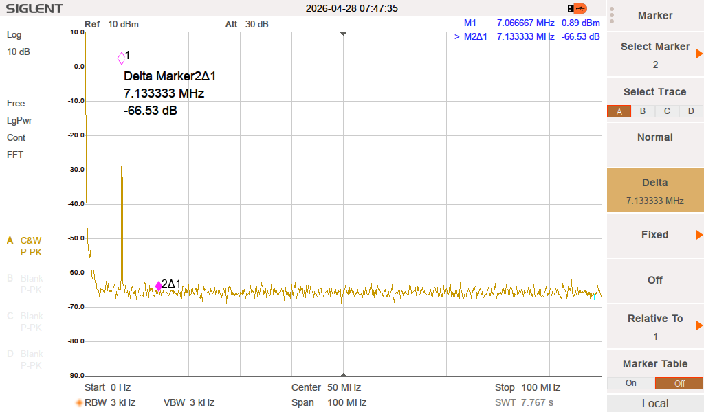
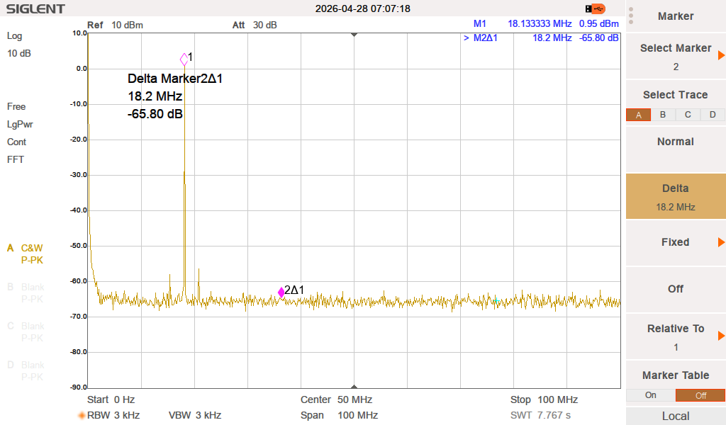
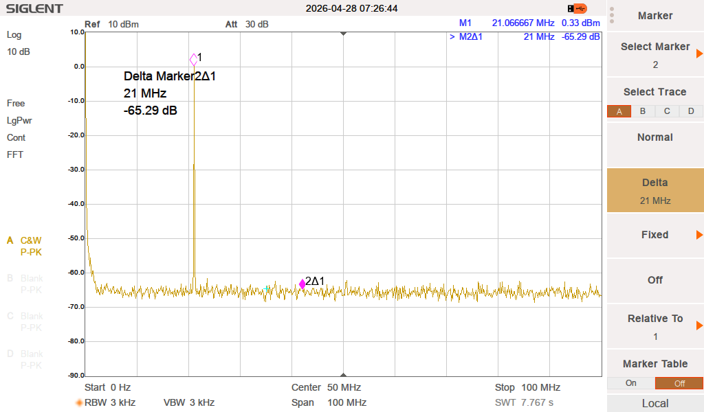
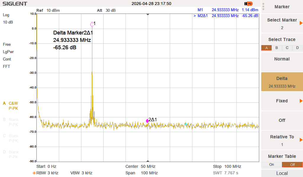
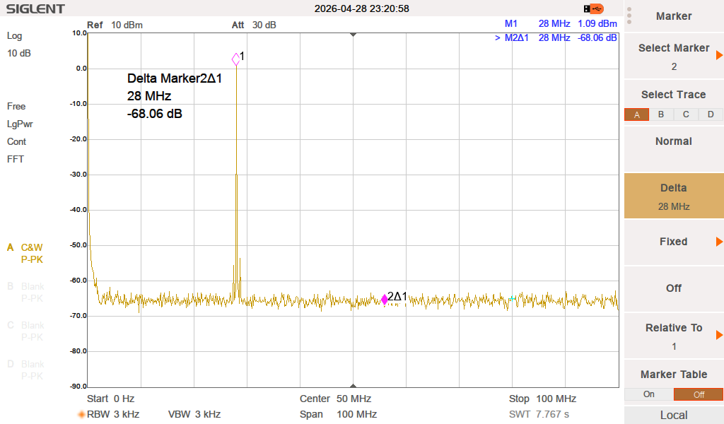
Measurement of Transmitter Harmonics
The following images show the spectrum of each band with a T41-3 radio set to 10 watts output in CW mode. This shows the primary function of the LPF which is the attenuation of transmitter harmonic energy. All bands show excellent rejection of transmitter harmonic energy. Note that some bands have some low frequency spurs around the carrier frequency. This is suspected to be from the Si5351, however, this has not been verified. These spurs change dramatically with carrier frequency, thus the suspected PLL source.
It is up to you, the builder of a transmitter, to verify that the spurious outputs meet the regulatory requirements in your country per whatever authority sets the limits. No information provided here implies the circuit designs will meet those requirements. Verify your transmitter performance before putting it on the air!