KF5N Radio Experimentation Site
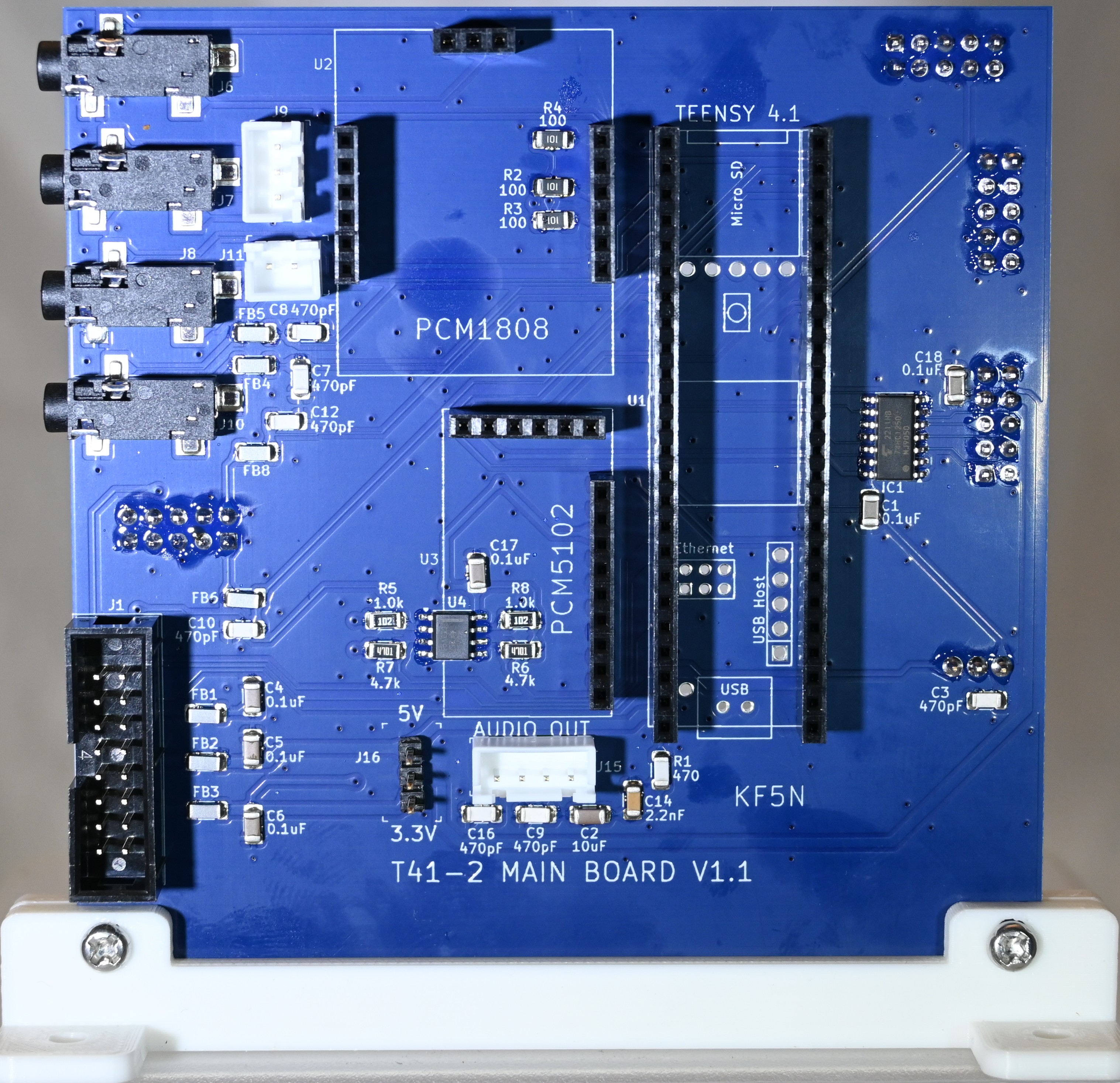
Main Board
T41-2 Main Board Version 1.2
This is the PCB for the T41-2 Main Board module for the T41 “Software Defined Transceiver”. The PCB was designed using the open-source design tool Kicad 8. The “teardrop” feature of the layout tool was used to increase PCB reliability.
The T41-2 Main Board evolved from the original V011 design. The Main Board is the central core of the T41 transceiver. This is where the DSP happens, user input is processed and the display graphics are generated. Input-output is very apparent on this board. There are a lot of connectors!
The board is technically easy to build, but it is very time consuming to build. A lot of work!
License
This design is licensed under the CERN Open Hardware Licence. A copy of the license is included in this repository. The license is also available via this link:
https://ohwr.org/cern_ohl_s_v2.txt
Summary of Main Board Design Features
The display buffer device is retained. The display buffer/driver device is required due to the required high-speed operation of the SPI bus between the Teensy and the display. The reason to use the driver device is that the Teensy’s “general purpose outputs” (GPOs) are weak. With a specified maximum output of 4mA, reliability of the SPI interconnect to the display cannot be guaranteed. Note that the Teensy is re-oriented on the board such that the wiring between the Teensy and driver device, and also between the output of the driver device and the display connector, is minimized. The display connector is moved to the bottom side of the board in order to minimize the length of the cable between the Main Board and the display.
A jumper is provided to select the display voltage of either 3.3 or 5.0 volts.
An I2C bus is routed to both power distribution connector J1 and also optionally via jumper resistors to the filter connector J3. Due to the loading inherent in the ribbon cables, an I2C “re-driver” device (U4) is added to the design. The re-driver is designed to handle a large amount of capacitive load. So far, testing indicates robust operation of the I2C bus with this device in place. It is planned to add I2C to other T41-2 modules in order to simplify interconnect. The re-driver device creates the foundation for the I2C expansion.
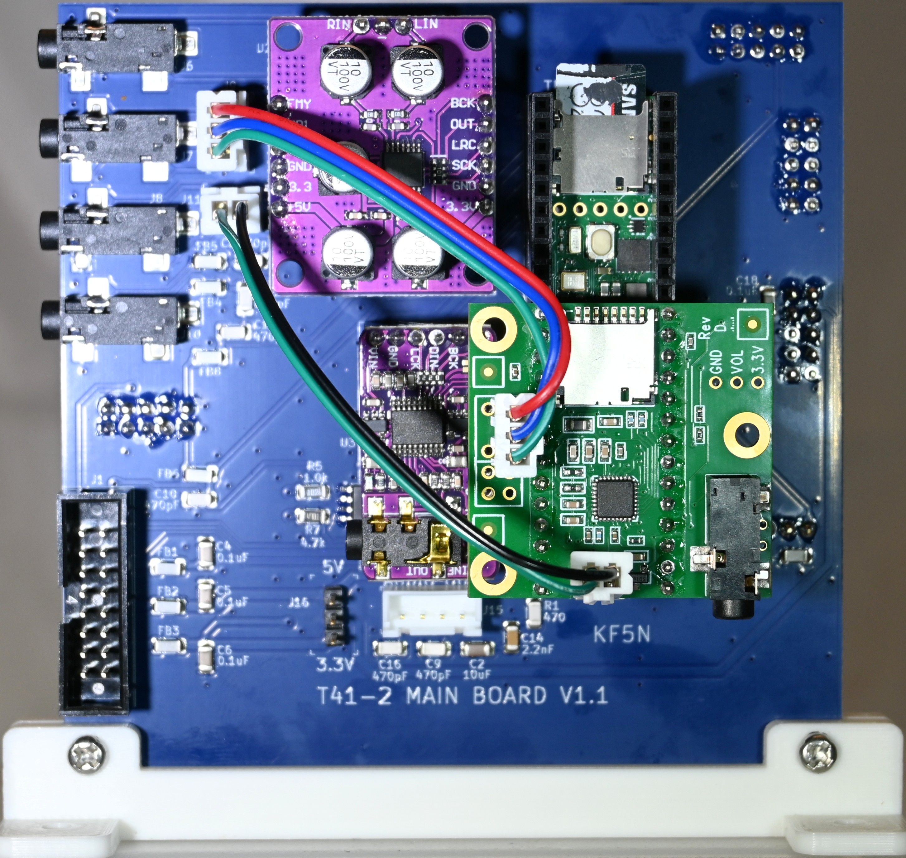
The Si5351 PLL device is removed. It is recommended to use an external Si5351 module instead. For more information, please refer to this repository:
https://github.com/Greg-R/bracket_dual_T41
Note that the QSE2DC/QSE2DCEZ boards include a connector to provide power and I2C to the Si5351 module. It should be easy to “hack” these connections to an older QSD or QSE board.
The same data converter modules, the PCM5102 and PCM1808, are retained. Pin spacing issues of the old Main Board have been resolved.
The audio amplifier is removed. A 4-pin connector is provided which includes audio out, amplifier enable, and ground. Design files for a 3D printed bracket for an off-the-shelf audio amplifier module are available here:
https://github.com/Greg-R/SDT_Case_KF5N/tree/main/bracket
The amplifier used in the KF5N T41 is available here:
https://www.amazon.com/gp/product/B07F596XMX
Of course, other audio amplifier modules can be used. Be sure to choose a module which includes an enable/disable control.
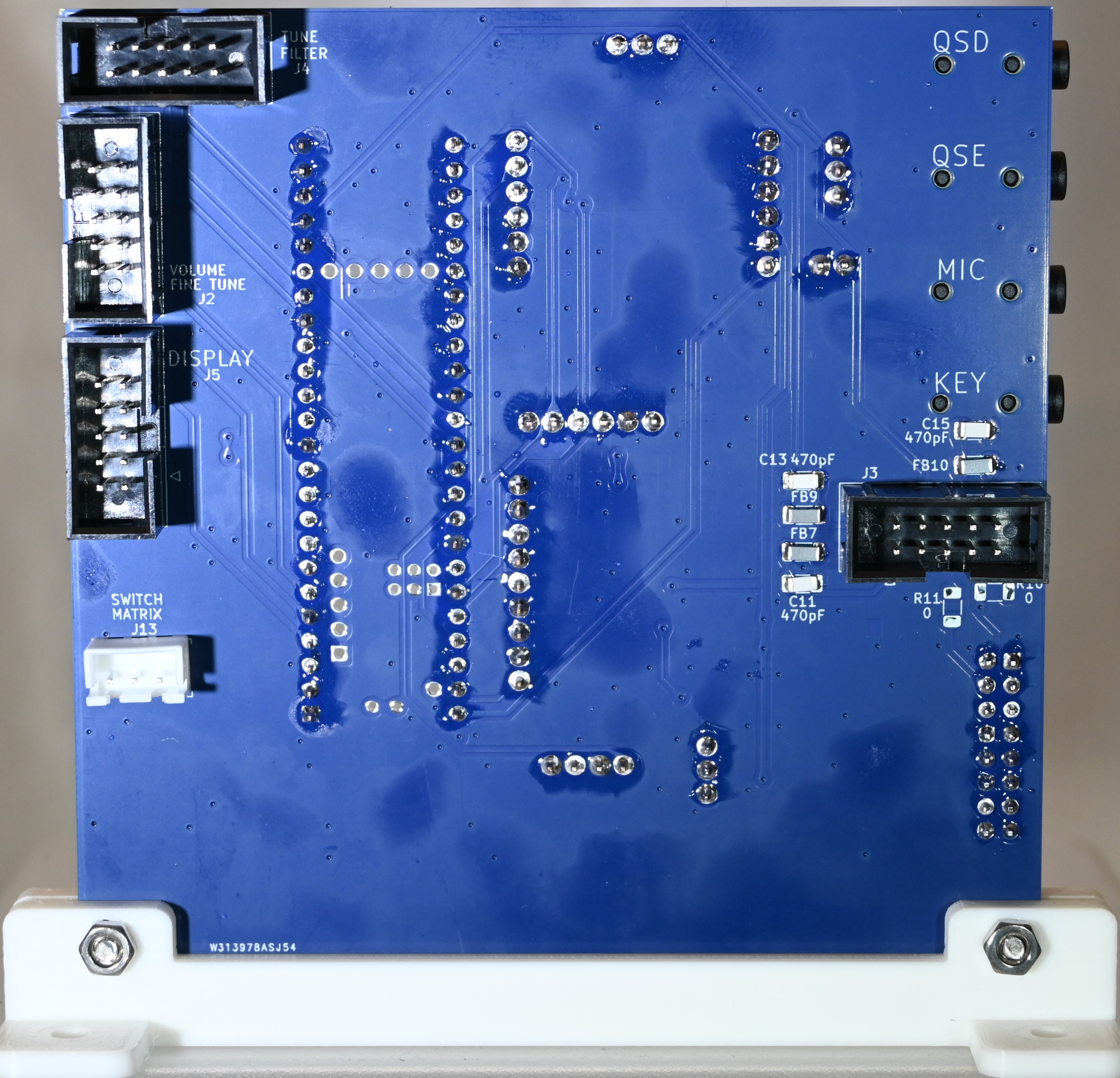
Interconnect to the radio modules and external hardware is fully covered. Here is a list of the interconnect:
- J1. Primary power distribution. Reset for QSD2 and QSE2 boards. TXRX signal. I2C bus replaces the speaker output of the original Main Board.
- J2: Volume and Fine Tune encoder connections.
- J3: Low-Pass Filter controls. This now includes I2C and power for future designs.
- J4: Tune and Filter encoder connections.
- J5: Display connector.
- J6: 3.5mm stereo connector to QSD.
- J7: 3.5mm stereo connector to QSE. If sideband is flipped, flip the connector at the Audio Adapter.
- J8: 3.5mm stereo connector to microphone. Tip is audio. Ring is PTT.
- J10: 3.5mm stereo connector to key. Tip is straight key and dit. Ring is dah.
- J13: Switch matrix. 3.3 volt reference from Teensy, input to Teensy ADC and ground.
- J15: Analog audio output and audio amplifier enable control.
- J16: Display power jumper, 3.3 or 5.0 volts.
Power supply decoupling (ferrite beads and bypass capacitors) have been added to critical interfaces. Perhaps one of the most critical is the Low Pass Filter interface. This interface is exposed to the full RF output power of the transmitter. This interface has been thoroughly decoupled with ferrite beads and shunt capacitors.
Gerber files for PCB fabrication are included in the gerbers folder. A PDF of the schematic is included for quick viewing of the circuit design in the doc folder.
T41EEE Arduino Sketch with Special Features for T41-2 Main Board
The Arduino sketch designed to work with the T41-2 Main Board is located here:
https://github.com/Greg-R/T41EEE
You will need to modify the file “MyConfigurationFile.h”. The default code looks like this:
// Set multiplication factors for your QSD and QSE boards.
#define MASTER_CLK_MULT_RX 4
#define MASTER_CLK_MULT_TX 4

// Uncomment this line for QSE2.
//#define QSE2
Assuming you are using both QSD2 and QSE2DCEZ, you should change the code to this:
// Set multiplication factors for your QSD and QSE boards.
#define MASTER_CLK_MULT_RX 2
#define MASTER_CLK_MULT_TX 2

// Uncomment this line for QSE2.
#define QSE2
To use the Si5351 module, there is another line to uncomment:
// Uncomment this line if using an external PLL module.
#define PLLMODULE
There are more changes required to use the external audio amplifier. The example below shows how the code should appear when using the T41-2 Main Board and the audio amplifier referenced above:
// Uncomment for the original T41 audio mute control.
//#define UNMUTEAUDIO LOW
//#define MUTEAUDIO   HIGH
// Use this for external amp with mute LOW, unmute HIGH.
#define UNMUTEAUDIO HIGH
#define MUTEAUDIO   LOW

// If using an external amplifier, the gain may need to be adjusted for the best volume range.
#define AUDIOSCALE  40    // A typical value is 20.  Increase or decrease this value depending on your amplifier gain.
Power Supply Decoupling and Regulators
The power supplies routed through the 16 wire ribbon cable are prone to noise, most likely from the Main board. Regulators for the three required voltages include low-esr bypass capacitors. This will provide clean bias sources to the modulator circuit. Series ferrite beads provide additional isolation and decoupling.
Connectors
The I/Q output connector is changed to surface mount. The RF SMA connectors are the same, or they can be changed to right-angle connectors to improve coaxial cable routing. The 16 pin IDC connector is the same as the V011 board.
PCB Layout
The PCB layout was completed using the open-source tool Kicad version 8.
Gerber files are included in the gerber folder. The prototype PCBs were fabricated by PCBWay at a cost of US$1.00 each. Shipping was about US$25.00 for quantity 5 boards. JLCPCB can be used, and has the option of cheaper, slower shipping.
Bill Of Material (BOM)
A public Digikey BOM is here:
https://www.digikey.com/en/mylists/list/CFS9I8P9OV
Please note that specific parts may or may not be available when attempting to order. It is the responsibility of the builder to find subsitutes as required.
Build Tips
In general, the T41-2 Main Board is easier to build than the original V010/V011 series boards. There are a few items to be aware of to avoid build errors. These are my observations. You may need to do things differently in your lab.
Be very careful when soldering connectors! Because when one of the through-hole connectors gets soldered in, they are very difficult to remove. I say this because there are connectors on BOTH sides of the board! The through-hole connectors will be towards the last, so make sure you are wide awake when they are soldered in.
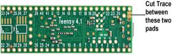
Important: Cut the trace on the Teensy!
There is a trace which must be sliced through in order to supply 5VDC to the Teensy from the Main Board. This is typically done via the USB connection. Since the radio is connected to USB only for programming, the 5VDC must come from the main board. Here is what the PJRC web page says:
VIN Pin When USB power is not used, 5V power may be applied to the VIN pin. Because VIN & VUSB are connected, power should not be applied to VIN while a USB cable is used, to prevent the possibility of power flowing back into your computer. Alternately, a pair of pads on the bottom side may be cut apart, to separate VUSB from VIN, allowing power to be safely applied while USB is in use.
Top Side Surface Mount Parts
This board doesn’t have a high density of surface mount parts. There are 2 integrated circuits, and a handful of capacitors, resistors, and ferrite beads. I have started using a hot plate to solder these parts. This goes quickly.
The four 3.5mm stereo jacks are surface mount and they are the last things to reflow. Keep an eye on them, and when they finally reflow, the top side reflow process is close to done.
There is a small marker to indicate Pin 1 on both of the ICs. They are both SOIC packages and solder easily without shorting.
Bottom Side Surface Mount Parts
I place these parts with solder paste as normal. Then I clamp the board in a vise, and use a hot air soldering tool to reflow the solder. You can do this quickly enough to not reflow the top side parts. There are only a few passive bottom side surface mount parts.
Headers for the Plug-in Devices
There are several headers for the Teensy and data converters. I happen to have a dead Teensy and data converters. I put the headers on the dead parts, and then insert the header pins into the Main board. This lines everything up nicely. No crooked headers! All of the pins are carefully hand soldered, which is a time consuming process.
IDC Connectors
As mentioned above, be sure to get these on the correct side of the board and oriented correctly! Take it very slow, and make sure the connectors are flush to the board during the soldering process.
Note that only the 16 pin IDC connector is on the top side of the board. The four 10 pin connectors are on the bottom side.
JST Connectors
There are 2, 3, and 4 pin JST connectors. I like to use these connectors, as they are polarized. Only the 3 pin Switch Matrix connector is inserted into the bottom side of the board. All others are mounted on the top side.
Header for Display Voltage Selection
The display voltage selection header is a regular style bare header with 3 pins. You will need to use a jumper to select the voltage which matches your display supply voltage.
Non-placed Parts
Don’t place R10 or R11. These connect the I2C bus to the Low Pass Filter Control connector. These may be used with future board designs.
Cable Assemblies
You will need to build several cables. This requires the small pins and a crimping device. The small pins come in a roll, and they are listed in the BOM. Here is a link to a crimper:
https://www.amazon.com/gp/product/B01N4L8QMW
The little cables are tedious to build. Proceed slowly and you will achieve a reliable result. A list of the cables which need to be built:
- 4 pin XH to (audio amplifer connector) audio amplifier. This carries analog audio and amplifier enable signals.
- 3 pin XH to 3 pin XH from Main Board to Audio Adapter. This is for transmit I and Q. Don’t use a polarized connector on the Audio Adapter side, because it may need to be flipped if the sideband is wrong. Use a plain header on the Audio Adapter so that flipping is possible.
- 2 pin XH to 2 pin XH from Main Board to Audio Adapter. This is for microphone audio.
- 3 pin XH to 3 pin XH from bottom side of Main Board to Switch Matrix.
High Resolution Photos of T41-2 Main Board
Links to photos of a fully constructed T41-2 Main Board follow. Click on the image for high-resolution photos.
PCB Symbols and Footprints
The libraries folder includes symbols and footprints. You will need these libraries:
https://github.com/Digi-Key/digikey-kicad-library
https://github.com/XenGi/teensy_library
https://github.com/XenGi/teensy.pretty
References and Further Reading
- “Digital Signal Processing and Software Defined Radio, Theory and Construction of the T41-EP Software Defined Transceiver”, by Albert F. Peter, AC8GY, and Dr. Jack Purdum, W8TEE. This is the ultimate resource for builders of the T41 Software Defined Transceiver: https://www.amazon.com/Digital-Signal-Processing-Software-Defined/dp/B0F5BDQZW3
- QSD2: https://github.com/Greg-R/qsd2
- QSE2: https://github.com/Greg-R/qse2
- QSE-Filter: https://github.com/Greg-R/QSE-Filter
- T41-2 Power Module: https://github.com/Greg-R/T41-2_Power
- Dual bracket and Si5351 external module: https://github.com/Greg-R/bracket_dual_T41
- T41EEE software for the T41 transceiver: https://github.com/Greg-R/T41EEE